28+ dual slope adc block diagram
With up to 8 GHz analog bandwidth 25 GSs sample rates standard 625 Mpts record length and a 12-bit analog to digital converter ADC the 6 Series MSO has the performance you need to capture waveforms with the best possible signal fidelity and resolution for seeing small waveform details. Block diagram of in-sensor analytics for detection of peaks and.
12 05 14cas2014 Adcs Dacs1 Cern Accelerator School Adcs And Dacs Analogue To Digital And Digital To Analogue Converters John Pickering Metron Designs Ppt Download
The analog input of most ADCs is 5V which is why nearly all signal conditioning front-ends provide a conditioned output that is the same.
. In this example CMS-4 readout is being used. Basics of dynamic element matching. The typical SAR ADC uses a sample-and-hold circuit that takes in the conditioned analog voltage from the signal conditioning front-end.
It consists of a successive approximation register SAR DAC and comparator. Multivibrators asymmetrical square wave generator bistable multivibrators monostable multivibrator sawtooth waveform generator triangular waveform generator. Differentiating and squaring the resulting data yields the slope of QRS peaks and prevents false peak detection associated with the T wave.
In order to obtain the relationship between the drain to source current I DS and its terminal voltages we divide characteristics in two regions of operation ie. 1A and Movie 1The M-Bot is composed of two fully inkjet-printed stretchable e-skin patches namely e-skin-R and e-skin-H which interface conformally with the robot and human skin respectively. Hence it is called a s dual slope A to D converter.
In dual slope type ADC the integrator generates two different ramps one with the known analog input voltage VA and another with a known reference voltage Vref. Multivibrators asymmetrical square wave generator bistable multivibrators monostable multivibrator sawtooth waveform generator triangular waveform generator. Carrier chip package with 28-pin.
Op amp comparators comparator as a. RS485 is an industry standard protocol for data transfer and provides numerous advantages. Typical conversion time is 100ns or less.
Typical Delta-Sigma ADC block diagram. Furthermore Symmetrical flexible SCs manufactured by PANI email protected demonstrated good cycle stability which was up to 87 for 10000 cycles at 5 mA cm 2. The output of SAR is given to n-bit DAC.
Enter the email address you signed up with and well email you a reset link. In this example CMS-4 readout is being used. To address these challenges we introduce here an artificial intelligence AIpowered human-machine interactive multimodal sensing robotic system M-Bot Fig.
The conversion of an analog input signal results in a corresponding 10-Bit digital number. Microelectronic Circuits 6th Edition - Adel S Sedra Kenneth Carless Smithpdf. Linear region and saturation region.
In linear region the I DS will increase linearly with increase in drain to source voltage V DS whereas in saturation region the I DS is. Op amp comparators comparator as a. The analog input of most ADCs is 5V which is why nearly all signal conditioning front-ends provide a conditioned output that is the same.
The optimized electrode had an ultra-high area capacitance of 48393987 mF cm 2 at 530 mA cm 2. Flash ADCs oversampling delta-sigma ADCs and DACsdiscrete and continuous-time integrators and circuit techniques. B Simplified sensor operating timing diagram for the dual-pixel-gain readout mode.
Associate membership to the IDM is for up-and-coming researchers fully committed to conducting their research in the IDM who fulfil certain criteria for 3-year terms which are renewable. Counter Type ADC Block Diagram Integrating Dual-Slope ADC. Sampling and sample-and-hold circuits quantization ADC and DAC metrics a survey ADC and DAC architectures.
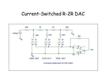
Counter type adc dual slope type adc flash type adc r 2r ladder dac successive approximation type adc. The equivalent analog output voltage of DAC VD is applied to the non-inverting input of the comparator. The block diagram of the proposed platform.
A universal VCO Board - MC100EL1648DG and PGA-103 A universal XCOPLL Board - NB3N501502511. Current steering and resistive DACs. Ideally the op amp amplifies only the difference in voltage between the two which is called the differential input voltageThe output voltage of the op amp V out is given by the equation where A OL is the open-loop gain of the amplifier the term.
Choosing the right OPAMP to drive an ADC SAR ADC Bipolar Voltage to Unipolar Voltage ADC Driver. 2The construction is simple and easier to design. Integrator waveform is started correspondingly counter starts counting from 0 to 2n-1 where n is the number of bits of ADC.
The amplifiers differential inputs consist of a non-inverting input with voltage V and an inverting input with voltage V. Each sensor consists of dual electrodes which act as a parallel plate capacitor with an intermediary dielectric layer in the form of the introduced. Choosing the right OPAMP to drive an ADC SAR ADC Bipolar Voltage to Unipolar Voltage ADC Driver.
The functional block diagram of successive approximation type of ADC is shown below. Counter type adc dual slope type adc flash type adc r 2r ladder dac successive approximation type adc. The diagram of the synthesis process was shown in Fig.
This converter lets you send and receive data using the RS485 network from your Arduino microcontroller. The Analog-to-Digital AD Converter module has 5-Channels for the 28-pin devices and 8-Channels for the 4044-pin devices. Typical SAR block diagram.
The logic diagram for the same is shown below. We provide assignment help in over 80 subjects. A universal VCO Board - MC100EL1648DG and PGA-103 A universal XCOPLL Board - NB3N501502511.
Dual Slope Analog to Digital Converter. 1It is the fastest type of ADC because the conversion is performed simultaneously through a set of comparators hence referred as flash type ADC. Typical SAR block diagram.
Similar to Serial TTL and RS232 interfaces the RS485 lets you transfer data between microcontrollers and devices but with extra features. Experience the performance difference. A 14-bit analog-to-digital converter ADC operating at a sampling frequency of 200 Hz digitizes the signals captured by each module.
This Article Discusses an Overview of Analog to Digital ADC Converter Block Diagram Designing Process Types Testing Its Applications. We are a leading online assignment help service provider. 4 - 0 - 0 - 0 - 8 - 12.
I-V Characteristics of PMOS Transistor. We will take care of all your assignment needs.
2
12 05 14cas2014 Adcs Dacs1 Cern Accelerator School Adcs And Dacs Analogue To Digital And Digital To Analogue Converters John Pickering Metron Designs Ppt Download
2
2
Cern Accelerator School Adcs And Dacs Analogue To
2
12 05 14cas2014 Adcs Dacs1 Cern Accelerator School Adcs And Dacs Analogue To Digital And Digital To Analogue Converters John Pickering Metron Designs Ppt Download

12 05 14cas2014 Adcs Dacs1 Cern Accelerator School Adcs And Dacs Analogue To Digital And Digital To Analogue Converters John Pickering Metron Designs Ppt Download
2
2
12 05 14cas2014 Adcs Dacs1 Cern Accelerator School Adcs And Dacs Analogue To Digital And Digital To Analogue Converters John Pickering Metron Designs Ppt Download

12 05 14cas2014 Adcs Dacs1 Cern Accelerator School Adcs And Dacs Analogue To Digital And Digital To Analogue Converters John Pickering Metron Designs Ppt Download

12 05 14cas2014 Adcs Dacs1 Cern Accelerator School Adcs And Dacs Analogue To Digital And Digital To Analogue Converters John Pickering Metron Designs Ppt Download
2
2
2
2